TEST INTERFACE BOARD
-
BOST Interface Solution Online Inquiry
Feature
Supply customized test solution
Speed X2 ~ X8
Parallel expansion
Command code interface
LUT pattern
Source sync & clock sync schem
Variable mode register setting
Multi firmware configuration
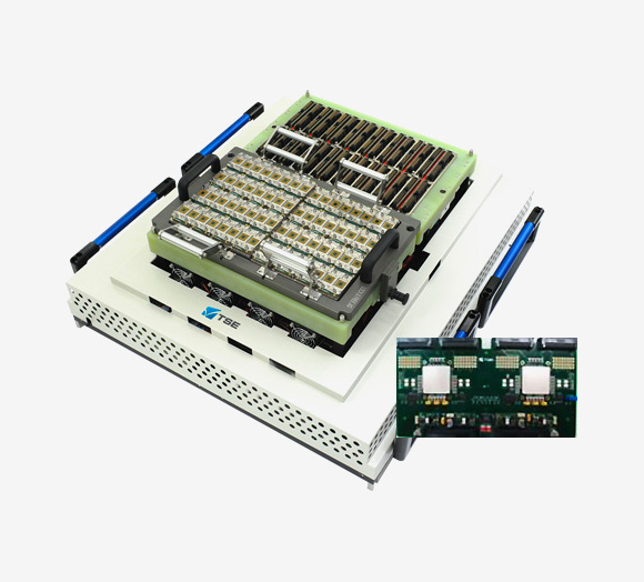
BOST is an optimal solution to suppress the rise of COT caused by increasing the speed and density of memory semiconductors. It will maximize productivity because it contributes to parallel expansion by testing the latest devices using old equipment without adding new facilities.
BOST Solution Development Experience
Target Tester Speed Benefit Application LPDDR2 T5581 / 85 800Mbps Speed up X2
Para ext x4AC, DC, IDD LPDDR2 Magnum 2X 1066Mbps Speed up X2
Para ext x4AC, DC, IDD DDR3 T5581 / 85 1Gbps Speed up X2
Para ext x4AC, DC, IDD DDR3 T5581 / 85 1600Mbps(DDR)
2133Mbps(SDR)Speed up x4~x8
Para ext x4AC, DC, IDD DDR4 T5581 / 85 1600Mbps(DDR)
2400Mbps(SDR)Speed up x4~x8
Para ext x4AC, DC, IDD eMCP
(LPDDR2 + eMMC)Magnum 2X 1066Mbps Speed up X2
Para ext x4 & ConcurrentAC, DC, IDD -
CFDS Interface Solution Online Inquiry
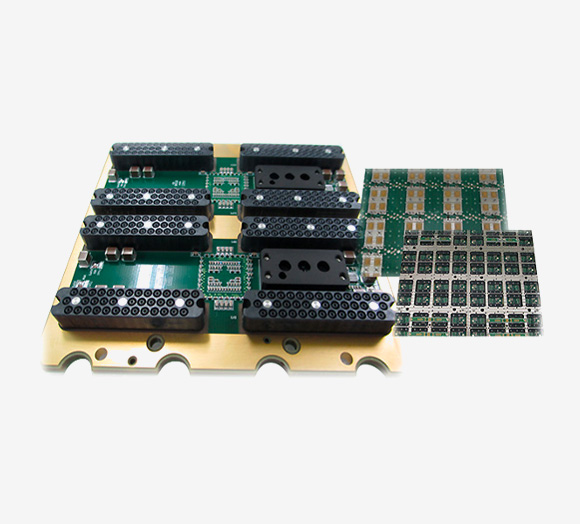
Feature
TE Application : T5581, T5585, T5588, T5593, T5503, Ultra Memory, Magnum
Target Device : DDR3, DDR4, LPDDR3, LPDDR4, GDDR5, GDDR6
Single Ended Input, Differential Output
Given the existing Low Speed Testers, the test environment requires a new high-speed tester as the CLK speed of memories(e.g. DDR3, DDR4, LPDDR3, LPDDR4, GDDR5, GDDR6) increases.
TSE’s CFDS interface solution utilizes existing a Low-Frequency Tester to realize High-Frequency Clock so that it can test a high-speed clock sync memory at a low cost without investing in a new tester.
-
Power Boost Interface Solution Online Inquiry
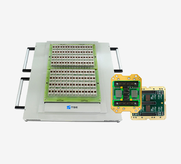
Feature
Test Device DDR3, DDR4, LPDDR3, LPDDR4, GDDR5 Input Voltage +2.5~5.5V Output Voltage +0.75~3.3V Output Current 2A Tracking Voltage +0.75~3.3V Accuracy ±5mV Thicker, thinner and more powerful devices are preferred for easy portability as the center of gravity moves from PC to smartphone.
Low-power DDR products are being developed as a way to reduce power consumption as memories evolve, and a low-power compensation Power Boost Interface Solution is being provided for testing low-power memory products.
company news


- Directions
- Headquarters (2nd Plant) 3rd plant MEMS Fab
TSE / 189, Gunsu 1-gil Jiksan-eup Seobuk-gu, Cheonan-si Chungcheongnam-do, Korea (213-15 Gunseo-ri) / TEL. +82 41-581-9955
(C) TSE Co., Ltd.
TOP