MEMS Product
mems product
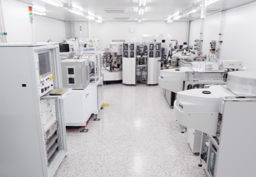
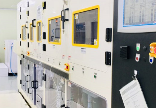
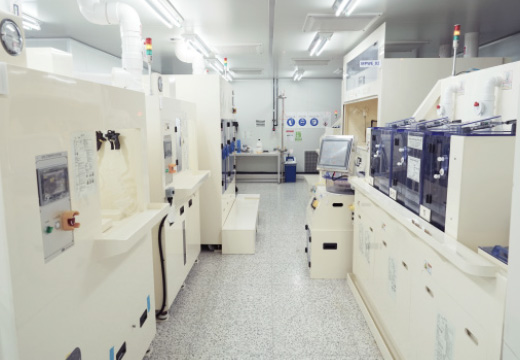
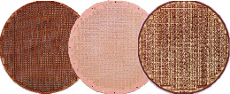
mems product Fab. Infrastructure
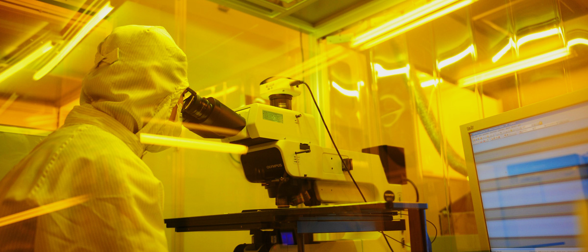
- All class 1000 clean room. (Class 100 @ PHOTO bay)
- Manufacturing equipment.
- Aligner, Electro Plate Bath, Sputter, Polisher, etc.
- Analysis equipment.
- FE-SEM, ICP, CVS, etc
- Measuring & Inspection equipment.
- 3D Vision, Alpha step, AOI, etc.
- Ceramic, Glass, Silicon wafers are possible.
- from 4” to 12” available.
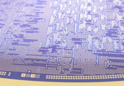
mems product MEMS Process
-
Thin Film
Able to make sub-micron thin film by Sputter or PECVD.
-
Photo
i-line & Broad band 1X Aligner.
Back & Front side align.
4”, 8”, 12” Process.
-
Electro Plating
EP bath for Ni, Ni alloy, Au, Cu, Sn, Rh.
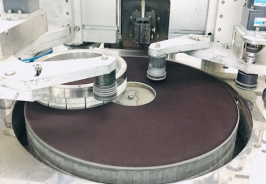
-
CMP
Polishing process for Ceramic & Silicon wafers.
-
ETCH
Wet etch process.
Dry(ICP) etch process.
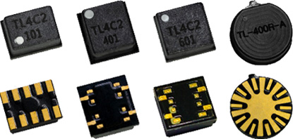
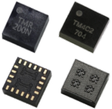
mems product MEMS Applications
- MEMS Structure
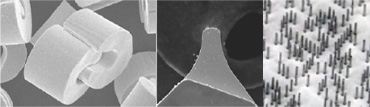
- Ceramic substrate
- MEMS Component
mems technology
-
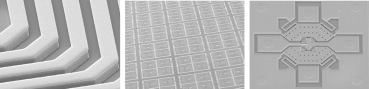
Sheet Type Multi-Layer Technology
Multi-layer simultaneous production
Channel sharing with multi-layer wiring
Enables high para probe card sharing with multi-layer wiring
Improved flatness of multi-layer
-
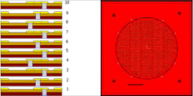
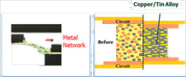
Interconnect Technology
Interconnect Technology with Conductive Ink
Electrical Connection by metal sintering
-
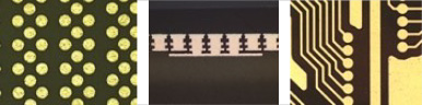
MEMS Thin Film Technology
Small Size Via : ≥ 15um
C4 Pad Pitch : ≥ 30um
-
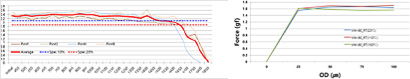
VPC Probe Technology
Low Contact Force : 1.45gf (@Force at OD 75um)
High CCC : 1,500mA (@ISMI)
Available Pitch : ≥ 50um
Long life cycle : ≥ 1,000,000TD

-
MEMS Probe Design and Fab. Technology
High reliability performance with new Ni alloy plating technology
MEMS Vertical Structure
Various probe solution for Cu-Pillar Bumps & BGA
High Aspect Ratio : 6.5:1
-
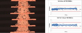
Stack-up Technology
Guaranteed thermal reliability : No Crack, No Delamination
(@TSCT, Reflow, Floating)Stable electrical characteristic : Resistance change within ±10%
(@Bare Board Test)
company news


- Directions
- Headquarters (2nd Plant) 3rd plant MEMS Fab
TSE / 189, Gunsu 1-gil Jiksan-eup Seobuk-gu, Cheonan-si Chungcheongnam-do, Korea (213-15 Gunseo-ri) / TEL. +82 41-581-9955
(C) TSE Co., Ltd.
TOP